| Title: | ATUMS 1-3: Highly luminescent Nanomaterial / Polymer Hybrids - Optoelectronic Materials |
| Partners: | University of Alberta, Edmonton, Canada & Technische Universität München TUM, Internationale Graduiertenschule für Funktionelle Hybridmaterialen (ATUMS), München, Germany |
| Funding: | funding through Deutsche Forschungsgemeinschaft DFG, Bonn, DFG IRTG 2022 "ATUMS" Project 1-3 |
| Duration: | 2015- |
| Contact: | Professor Dr. Bernhard Rieger, Technische Universität München (TUM), Fakultät für Chemie WACKER-Lehrstuhl für Makromolekulare Chemie, Garching |
| Homepage: | https://www.makro.ch.tum.de/index.php?id=3005&L=1http://www.dfg.de/foerderung/programme/listen/projektdetails/index.jsp?id=245845833 |
IRTG 2022 "ATUMS" - Project 1-3 1-3:
Highly luminescent Nanomaterial/Polymer Hybrids
TUM: Markus Becherer, Bernhard Rieger, Thomas Fässler, Paolo Lugli
UofA: Frank Hegmann, Jonathan Veinot
Doctorial Candidates: Alina Lyuleeva, Tobias Helbich, Regina Sinelnikov, Mary A. Narreto
Silicon Nanosheets (SiNSs) based composites show outstanding (opto)electronic properties, as already published within the framework of this project [ATUMS 1-3] [1-4].
Furthermore, they are exploit for temperature or humidity sensors, currently investigated at the Chair of Nanoelectronics (Technical University of Munich).
In order to optimize SiNSs for real-world sensor applications, we will concentrate not exclusively on synthesis, characterization and deposition of SiNSs, but also on engineering tasks as given in detail below. Using various facilities and the expertise of the groups at the Technical University of Munich (TUM) and the University of Alberta (UofA, Canada), the ATUMS members can develop close collaboration for an efficient progress in their research.
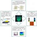
From crystalline Calcium Disilicide (CaSi2) in the group of Prof. Rieger (TUM) synthesized and with a variety of different molecules functionalized SiNSs will be deposited by different methods (spin-coating, dip-coating, spray-coating) and characterized in detail by e.g., atomic force microscopy (AFM), photoluminescence (PL) and time-resolved PL, Fourier transform infrared (FTIR) and energy-dispersive X-ray (EDX) spectroscopy.
Here, we will intensely profit from the expertise of the other groups in Chemistry and Physics within the ATUMS collaboration.
The interesting (opto)electronic properties of the SiNSs, such as green PL, will be closely investigated.
Together with the group of Prof. Frank Hegmann (UofA), we will explain the origin of the PL and the processes, which take place during the de-excitation.
With the surface modification of the SiNSs, their dispersibility in different solvents can be optimized, which is the basis for homogeneous blend formation.
Subsequently, these materials can be applied for the fabrication of e.g. optimized and enhanced field-effect transistors (FETs), which are based on SINSs and semiconducting polymer based blends.
This application field of the nanosized two-dimensional silicon is one of the ongoing studies in our groups.
In this connection, also electron paramagnetic resonance (EPR) measurements will be carried out together with the co-workers of the Physics department and the Walter Schottky Institute (TUM), especially with the group of Prof. Stutzmann (TUM).
The EPR measurements will allow us to look deeper into the light exposure impact on the material and to understand the occurring charge transfer processes within the as prepared blends.
Furthermore, schemes for resistless lithography (e.g. laser written shadow masks) will be employed to contact the functionalized SiNSs by conventional Cr/Au contacts and/or spray deposited carbon nanotubes (CNTs), silver nanowires (AgNWs) and/or copper nanowires (CuNWs).
The shadow masks will provide contact patterns through which conductive and semi-transparent electrodes will be deposited.
Resistless techniques have the advantage of not altering the device under test in an additive deposition step, keeping the substrate clean at the same time.
For the electrical measurements of the fabricated devices, conductive AFM or Electron-beam lithography, followed by metal evaporation for contact pads will be considered.
We will develop schemes for the application of the SiNSs, in specific “arrays” to harvest their properties and optimize them in terms of efficiency, low drift, reliability and endurance.
The synthesized SiNSs can be deposited as flakes, forming random patterns and networks on the substrate.
However, for the optimization of the electrical contact geometry, micron-sized spacing of interdigitating contacts or incorporating SiNSs into a nanowire network could allow to measure and harvest the SiNSs film properties.
A further aim of this project is to optimize the SiNSs as a potential sensor material by e.g., building a demonstrator platform, or integrating them into conventional discrete electronic circuitry, such as electronic modulation/demodulation as efficient noise suppression technique.
Furthermore, Wheatstone bridges for differential resistance measurement and encapsulated reference sensors for temperature and drift compensations can be developed.
Additionally, another goal is to understand the aging processes of SiNSs based devices and to optimize prospective encapsulation techniques.
By temperature assisted, accelerated ageing experiments in a controlled environment (e.g., climatic chamber, vacuum, inert gas), SiNSs devices will be proven for their “industrial” applications.
[1] T. Helbich, A. Lyuleeva et al. Chemistry - A European Journal, 2016, 22, 18, 6194–6198.
[2] T. Helbich, A. Lyuleeva et al. Adv. Funct. Mater., 2016, 26, 6711–6718
[3] A. Lyuleeva, T. Helbich et al. Journal of Physics D: Applied Physics, 2017, 50, 13, 8pp.
[4] T. Helbich, A. Lyuleeva et al. Adv. Funct. Mater., 2017, 1606764.


