CMOS without dopants: Reconfigurable Silicon Nanowire Transistors


Over the past 30 years electronic applications have been dominated by complementary metal oxide semiconductor (CMOS) devices. These combine p- and n-type field effect transistors (FETs) to reduce static power consumption.
However, CMOS transistors are limited to static electrical functions, i.e., electrical characteristics that cannot be changed.
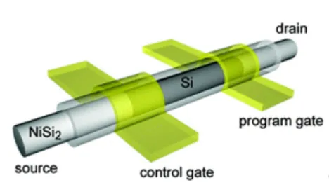
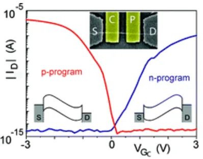
Here we present the concept and a demonstrator of a universal transistor that can be reversely configured as p-FET or n-FET simply by the application of an electric signal. This concept is enabled by employing an axial nanowire heterostructure (metal/intrinsic-silicon/metal) with independent gating of the Schottky junctions. In contrast to conventional FETs, charge carrier polarity and concentration are determined by selective and sensitive control of charge carrier injections at each Schottky junction, explicitly avoiding the use of dopants as shown by measurements and calculations.
Besides the additional functionality, the fabricated nanoscale devices exhibit enhanced electrical characteristics, e.g., record on/off ratio of up to 1 × 10⁹ for Schottky transistors. This novel nanotransistor technology makes way for a simple and compact hardware platform that can be flexibly reconfigured during operation to perform different logic computations yielding unprecedented circuit design flexibility.
Dopants in advanced CMOS Nano-transistors introduce intrinsic device parameter fluctuations which are detrimental to circuit performance. Therefore the development of dopant-free transistors like demonstrated in this work, should be beneficial for further scaling.
The paper has just been published in Nano Letters
An extension and application of this will be shown by EPFL researchers at the IEDM 2012 in the paper:
(Paper #8.4, “Polarity Control in Double-Gate, Gate-All-Around Vertically Stacked Silicon Nanowire FETs,” M. De Marchi et al, EPFL)