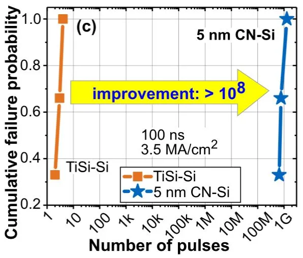
Scalability down to 5 nm demonstrated:
check it out:
https://ieeexplore.ieee.org/abstract/document/8624356
pdf: https://ieeexplore.ieee.org/stamp/stamp.jsp?tp=&arnumber=8624356
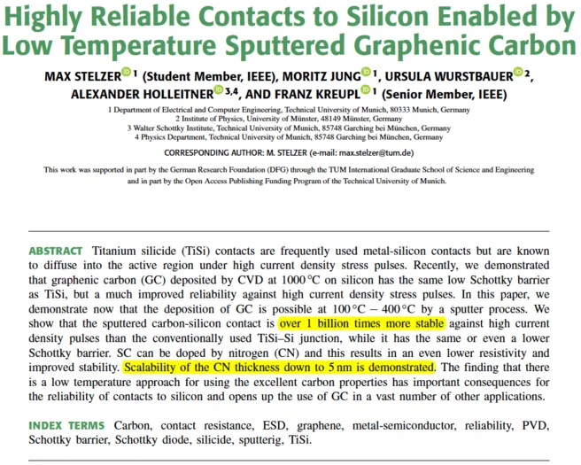
ABSTRACT Titanium silicide (TiSi) contacts are frequently used metal-silicon contacts but are known to diffuse into the active region under high current density stress pulses. Recently, we demonstrated that graphenic carbon (GC) deposited by CVD at 1000 °C on silicon has the same low Schottky barrier as TiSi, but a much improved reliability against high current density stress pulses. In this paper, we demonstrate now that the deposition of GC is possible at 100 °C – 400 °C by a sputter process. We show that the sputtered carbon-silicon contact is over 1 billion times more stable against high current density pulses than the conventionally used TiSi–Si junction, while it has the same or even a lower Schottky barrier. SC can be doped by nitrogen (CN) and this results in an even lower resistivity and improved stability. Scalability of the CN thickness down to 5 nm is demonstrated. The finding that there is a low temperature approach for using the excellent carbon properties has important consequences for the reliability of contacts to silicon and opens up the use of GC in a vast number of other applications.
INDEX TERMS Carbon, contact resistance, ESD, graphene, metal-semiconductor, reliability, PVD,Schottky barrier, Schottky diode, silicide, sputterig, TiSi
UPDATE April 2019: Our paper is #9 of most downloaded paper in March 2019
https://ieeexplore.ieee.org/xpl/topAccessedArticles.jsp?punumber=6245494&topArticlesDate=March +2019
UPDATE June 2019: Our paper is #11 of most downloaded paper in May 2019
https://ieeexplore.ieee.org/xpl/topAccessedArticles.jsp?punumber=6245494&topArticlesDate=May+2019
UPDATE July 2019: Our paper is #35 of most downloaded paper in June 2019
https://ieeexplore.ieee.org/xpl/topAccessedArticles.jsp?punumber=6245494&topArticlesDate=June %202019

